August 16, 2021
The vast majority of amplifiers can be driven with the same voltage driving the input and output stages of the amplifier. In most common amplifier architectures, the supplies for the input and output stages are internally connected; however, on some Apex power amplifiers these pins are separated to allow a higher voltage to be applied to the input stage; a feature which can increase output swing and improve overall amplifier efficiency. The voltages applied to these pins are referred to as “Boost Voltage” and “Supply Voltage” for the input and output stages respectively. Because circuit designs implementing Boost Supplies come with the tradeoff of additional costs this feature is recommended for applications where a single set of supplies does not provide adequate system performance. This Tech Talk will highlight the benefits of incorporating boost supplies into applications where maximized amplifier performance and efficiency are key.
To evaluate the use of Boost Supplies via real world example we will focus on Apex’s PA05 power amplifier which has excellent current capabilities, high internal power dissipation, and can be configured to take advantage of Boost Supplies.
For our first example we will review an application that requires driving a mostly resistive load of 1.5ohms with a pulsed 1kHz sine wave that is 85VPP centered at 0V. The output will be pulsed for 100ms then sit at zero for 900ms, giving it a 10% duty cycle to limit power dissipation. Because this load is resistive, the voltage and current are both in phase, which is the worst-case scenario for voltage swing because current and output voltage will peak at the same time. The peak current can be found by using the peak voltage and dividing it by the load resistance, resulting in a 28.3A peak.
A brief review of Figure 1 below illustrates that the PA05 is limited to 100V across +Vs to –Vs

Figure 1: From PA05 Datasheet
With our example application’s target of 85Vpp on the output, the supply voltage would need to exceed its 100V absolute maximum in order to eliminate clipping, which could not be achieved without damaging the amplifier.
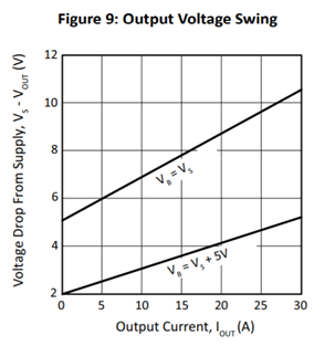
Figure 3: From PA05 Datasheet
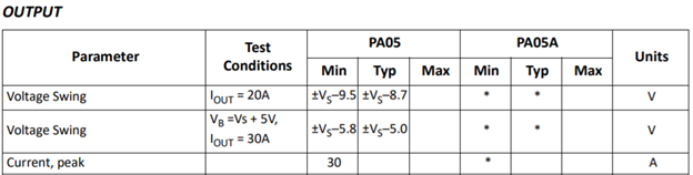
Figure 3 to the left confirms this, indicating that 28A of output current on the VB = VS curve requires more than 10V of supply overhead on each rail in addition to the desired 85Vpp output. Figure 4A shows the utilization of maximum supplies applied to the PA05, but with insufficient headroom to properly swing the output. This results in the waveform seen in Figure 5, where the sine wave’s peaks and troughs are clipped, and the output is heavily distorted.
| A | B |
 |
 |
Figure 4: Supply Configuration without and with boost supplies
The configuration seen in Figure 4B shows the addition of Boost Supplies each 5V above and below the VS supplies as described in Figure 2. According to the table in Figure 2, this enables the PA05 output to swing significantly closer to the supply rail. By creating a 5V difference between the boost and supply voltage pins, the voltage swing increases to within 5V of each rail while delivering 30A. +50V and -50V for +Vs and -Vs respectively, and +55V and -55V for +VB and -VB are sufficient to provide an 85Vpp sine wave with no clipping as indicated by the dashed line seen in Figure 5. It is also worth noting that the additional 55V supplies only need to source current up to 100mA instead of the 28.3A peak required by the load; that burden remains on the ±Vs supplies. The 100mA is the quiescent current that is required by input stage of the amplifier to operate. (also listed in the PA05 datasheet).
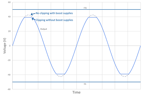
Figure 5: Plot of output and supply rails
For high current applications design engineers are presented with two options: the use of a switching (PWM) amplifier or a linear amplifier. Switching amplifiers offer superior efficiency but come with the drawback of significant switching noise, whereas linear amplifiers offer excellent signal fidelity but can often run into power limitations when used for high power applications. In applications where additional signal noise cannot be tolerated the engineer must use a linear amplifier, in such applications the use of Boost Supplies offers significant advantages in the reduction of the amplifier’s internal power dissipation, alternatively it can enable the engineer to drive greater loads with an equivalent internal power dissipation.
To put this into a real-world example, we will again reference the PA05 and take a mostly resistive load of 750mΩ that needs to be driven continuously with a 1kHz sine wave at 40VPP centered around 0V. The peak current required to drive this load is 26.7A, so according to Figure 3, over 10V of headroom is required utilizing only the VS pins. To drive the load with minimal distortion, +/- 31V supplies are needed as seen in Figure 6A below.
|
|
A 750mΩ load being driven with a 40Vpp sine wave will dissipate approximately 267W of power with the amplifier itself consuming an additional 267W of power internally!
According to Figure 1, this exceeds the maximum power dissipation for the package which would impose extraordinary heatsinking requirements. Continuing with the theme of this Tech Talk, let’s fix this by adding boost supplies.
From the first example, adding 5V worth of boost supplies allows us to reduce our headroom from >8V from the rail to closer to 5V. The new supply set up can be seen in Figure 6B and the change in headroom without distortion is represented graphically in Figure 7. With this new configuration, the internal power dissipation is reduced to 182W, with a total power savings of 85W! This lower power dissipation also helps alleviate some of the challenge faced with heatsink implementation.
|
|
|
|
The Apex Power Design Software Tool is designed to identify suitable parts for systems ranging from simple to more complex and helps automate many of the calculations required when working with high power linear and PWM amplifiers.
Download the Apex Power Design Software Tool here!
Back